

This English question involves literary analysis, grammar, or writing skills. The detailed response below provides a well-structured answer with supporting evidence and clear explanations.
ScanSolve AI Answer
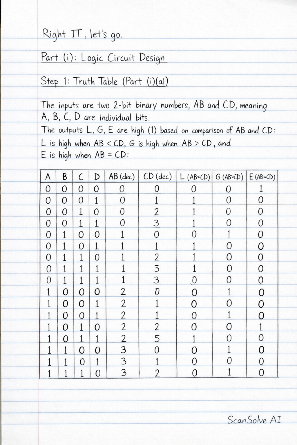
Part (i): Logic Circuit Design Step 1: Truth Table (Part (i)(a)) The inputs are two 2-bit binary numbers, AB and CD, meaning A, B, C, D are individual bits. The outputs L, G, E are high (1) based on the comparison of AB and CD: L is high when AB < CD, G is high when AB > CD, and E is high when AB = CD. |c|c|c|c|c|c|c|c|c| A & B & C & D & AB (dec) & CD (dec) & L (AB<CD) & G (AB>CD) & E (AB=CD) \\ 0 & 0 & 0 & 0 & 0 & 0 & 0 & 0 & 1 \\ 0 & 0 & 0 & 1 & 0 & 1 & 1 & 0 & 0 \\ 0 & 0 & 1 & 0 & 0 & 2 & 1 & 0 & 0 \\ 0 & 0 & 1 & 1 & 0 & 3 & 1 & 0 & 0 \\ 0 & 1 & 0 & 0 & 1 & 0 & 0 & 1 & 0 \\ 0 & 1 & 0 & 1 & 1 & 1 & 0 & 0 & 1 \\ 0 & 1 & 1 & 0 & 1 & 2 & 1 & 0 & 0 \\ 0 & 1 & 1 & 1 & 1 & 3 & 1 & 0 & 0 \\ 1 & 0 & 0 & 0 & 2 & 0 & 0 & 1 & 0 \\ 1 & 0 & 0 & 1 & 2 & 1 & 0 & 1 & 0 \\ 1 & 0 & 1 & 0 & 2 & 2 & 0 & 0 & 1 \\ 1 & 0 & 1 & 1 & 2 & 3 & 1 & 0 & 0 \\ 1 & 1 & 0 & 0 & 3 & 0 & 0 & 1 & 0 \\ 1 & 1 & 0 & 1 & 3 & 1 & 0 & 1 & 0 \\ 1 & 1 & 1 & 0 & 3 & 2 & 0 & 1 & 0 \\ 1 & 1 & 1 & 1 & 3 & 3 & 0 & 0 & 1 \\ Step 2: Boolean Expressions (Part (i)(b)) Using comparator logic, the simplified Boolean expressions for L, G, and E are: E = (A XNOR C) · (B XNOR D) L = A'C + (A XNOR C)B'D G = AC' + (A XNOR C)BD' Step 3: Circuit Diagram (Part (i)(c)) The circuit diagram is constructed using standard logic gates based on the Boolean expressions. Let X_AC = A XNOR C and X_BD = B XNOR D. For E: An AND gate takes X_AC and X_BD as inputs. For L: An AND gate takes A' (NOT A) and C as inputs. Another AND gate takes X_AC, B' (NOT B), and D as inputs. An OR gate takes the outputs of these two AND gates as inputs. For G: An AND gate takes A and C' (NOT C) as inputs. Another AND gate takes X_AC, B, and D' (NOT D) as inputs. An OR gate takes the outputs of these two AND gates as inputs. This circuit requires two XNOR gates, four NOT gates, five AND gates, and two OR gates. Part (ii): 8-bit 2's Complement and Logic Gates Step 4: 8-bit 2's Complement Computations (Part (ii)(a)) -35 + (-11) Convert 35_10 to 8-bit binary: 00100011_2. 2's complement of 35_10 (for -35_10): 11011101_2. Convert 11_10 to 8-bit binary: 00001011_2. 2's complement of 11_10 (for -11_10): 11110101_2. Add the 2's complement numbers: r 11011101_2 (-35_10) \\ + 11110101_2 (-11_10) \\ 111010010_2 (-46_10) Discard the carry-out. The 8-bit result is 11010010_2. 19 - (-4) This is equivalent to 19 + 4. Convert 19_10 to 8-bit binary: 00010011_2. Convert 4_10 to 8-bit binary: 00000100_2. Add the binary numbers: r 00010011_2 (19_10) \\ + 00000100_2 (4_10) \\ 00010111_2 (23_10) The 8-bit result is 00010111_2. Step 5: Hexadecimal Addition (Part (ii)(b)) Add (93)_16 and (DE)_16: r 93_16 \\ + DE_16 \\ Rightmost column: 3 + E = 3 + 14 = 17_10. This is 1_16 with a carry of 1. Leftmost column: 9 + D + 1 (carry) = 9 + 13 + 1 = 23_10. This is 7_16 with a carry of 1. Final carry: 1. The sum is 171_16. Step 6: Generate NOT and OR gates using NAND gates ONLY (Part (ii)(c)) NOT gate using NAND gates: A NOT gate can be created by connecting both inputs of a NAND gate to the same input signal. If the input is A, the output is (A · A)' = A'. A NAND A' OR gate using NAND gates: An OR gate can be created using three NAND gates, based on De Morgan's theorem: A + B = (A' · B')'. 1. Invert input A using a NAND gate to get A'. 2. Invert input B using a NAND gate to get B'. 3. Feed A' and B' into a third NAND gate. The output will be (A' · B')' = A'' + B'' = A + B. rcl A & & NAND A' \\ B & & NAND B' \\ A' & & NAND A+B \\ B' & & What's next? Send 'em!