

This computer science problem involves algorithmic thinking and programming concepts. The solution below explains the approach, logic, and implementation step by step.
ScanSolve AI Answer
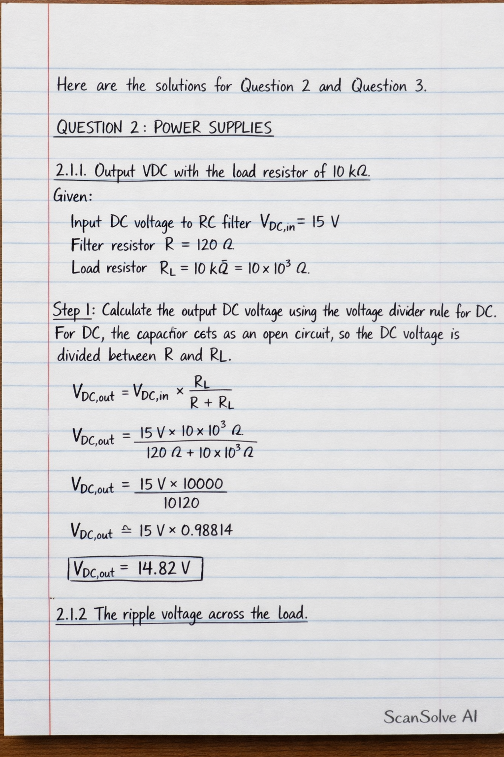
Here are the solutions for Question 2 and Question 3. QUESTION 2: POWER SUPPLIES 2.1.1 Output VDC with the load resistor of 10 k Given: Input DC voltage to RC filter V_DC,in = 15 V Filter resistor R = 120 Load resistor R_L = 10 k = 10 × 10^3 Step 1: Calculate the output DC voltage using the voltage divider rule for DC. For DC, the capacitor acts as an open circuit, so the DC voltage is divided between R and R_L. V_DC,out = V_DC,in × (R_L)/(R + R_L) V_DC,out = 15 V × (10 × 10^3 )/(120 + 10 × 10^3 ) V_DC,out = 15 V × (10000)/(10120) V_DC,out ≈ 15 V × 0.98814 V_DC,out = 14.82 V 2.1.2 The ripple voltage across the load Given: Input peak-to-peak ripple voltage V_r(pp),in = 1.5 V Line frequency f_line = 50 Hz Filter resistor R = 120 Filter capacitor C = 150 F = 150 × 10^-6 F Load resistor R_L = 10 k = 10 × 10^3 Step 1: Calculate the ripple frequency for a full-wave rectifier. f_r = 2 × f_line = 2 × 50 Hz = 100 Hz Step 2: Calculate the capacitive reactance X_C at the ripple frequency. X_C = (1)/(2 f_r C) = (1)/(2 (100 Hz)) (150 × 10^-6 F) X_C = (1)/(0.03) ≈ 10.61 Step 3: Calculate the equivalent impedance of the parallel combination of C and R_L. Since R_L X_C, the parallel impedance is approximately X_C. |Z_eq| = (R_L X_C)/(sqrt(R_L^2 + X_C^2)) = ((10 × 10^3 ) × 10.61 )/(sqrt((10 × 10^3 )^2 + (10.61 )^2)) |Z_eq| ≈ 10.61 Step 4: Calculate the output ripple voltage using the AC voltage divider rule. V_r(pp),out = V_r(pp),in × |Z_eq|sqrt(R^2 + |Z_eq)|^2 V_r(pp),out = 1.5 V × (10.61 )/(sqrt((120 )^2 + (10.61 )^2)) V_r(pp),out = 1.5 V × (10.61)/(sqrt(14400 + 112.57)) V_r(pp),out = 1.5 V × (10.61)/(120.47) V_r(pp),out ≈ 0.132 V 2.1.3 The percentage ripple factor of the first capacitor Given: Peak-to-peak ripple voltage across the first capacitor V_r(pp) = 1.5 V DC voltage across the first capacitor V_DC = 15 V Step 1: Calculate the RMS ripple voltage. For a triangular ripple, V_r(rms) = V_r(pp)2sqrt(3). V_r(rms) = 1.5 V2sqrt(3) ≈ (1.5)/(3.464) ≈ 0.433 V Step 2: Calculate the percentage ripple factor. Percentage ripple factor = V_r(rms)V_DC × 100\% Percentage ripple factor = 0.433 V15 V × 100\% Percentage ripple factor = 2.89% 2.2 Briefly describe the operational principle of a voltage tripler. A voltage tripler is a type of voltage multiplier circuit that converts an AC input voltage into a DC output voltage that is approximately three times the peak value of the AC input. It achieves this by using a network of diodes and capacitors. During different half-cycles of the AC input, capacitors are charged in parallel to the peak input voltage. These charged capacitors are then effectively connected in series with each other and the input voltage, allowing their voltages to sum up and produce a higher DC output voltage. 2.3 Draw a neat, labelled circuit diagram of a Zener-diode reference source. A Zener diode reference source typically consists of a series current-limiting resistor (R_S) connected to an unregulated DC input voltage (V_in). A Zener diode is then connected in parallel with the output (and the load R_L), with its cathode connected to the positive side of the output and its anode to the negative side. The Zener diode maintains a constant voltage (V_Z) across the load, provided the input voltage is sufficiently high and the current through the Zener diode is within its operating range. (Diagram cannot be rendered in text. It would show a voltage source V_in, a series resistor R_S, and a Zener diode in parallel with a load resistor R_L, with the Zener diode's cathode connected to the positive output and anode to ground.) QUESTION 3: AMPLIFIERS 3.1 Explain the term, stabilisation. In electronics, stabilisation refers to the process of maintaining a circuit's desired operating conditions or output characteristics constant despite variations in external factors. For an amplifier, this typically means keeping its Q-point (quiescent operating point) stable against changes in temperature, supply voltage, or component tolerances, ensuring consistent gain and preventing issues like thermal runaway. 3.2 Calculate the value of the base resistor with the aid of precise method if the following information about the transistor is known: Given: Amplifier input impedance Z_in = 2.5 k = 2500 Transistor h-parameters: h_ie = 13 k = 13000 h_re = 2.8 × 10^-4 h_fe = 300 Collector resistor R_C = 480 Load resistor R_L = 6 k = 6000 Source resistance R_S = 0 Step 1: Calculate the effective load resistance R_L' seen by the collector. R_L' = R_C || R_L = (R_C × R_L)/(R_C + R_L) R_L' = (480 × 6000 )/(480 + 6000 ) = (2880000)/(6480) ≈ 444.44 Step 2: Calculate the input impedance looking into the base of the transistor (Z_in(base)). For a common-emitter configuration, Z_in(base) = h_ie + h_re h_fe R_L'. Z_in(base) = 13000 + (2.8 × 10^-4) × 300 × 444.44 Z_in(base) = 13000 + 0.084 × 444.44 Z_in(base) = 13000 + 37.33 = 13037.33 Step 3: Calculate the base resistor R_B. For a fixed bias common-emitter amplifier, the overall input impedance of the amplifier stage is Z_in = R_B || Z_in(base). Z_in = R_B × Z_in(base)R_B + Z_in(base) Rearranging for R_B: R_B = Z_in × Z_in(base)Z_in(base) - Z_in R_B = (2500 × 13037.33 )/(13037.33 - 2500 ) R_B = (32593325)/(10537.33) R_B ≈ 3093.1 3.3 Calculate the output voltage for an integrator operational amplifier. Given: Input signal V_in is a square waveform of ± 2 V. Frequency f = 800 Hz. Input resistor R_in = 10 M = 10 × 10^6 . Feedback capacitor C_f = 0.01 F = 0.01 × 10^-6 F = 1 × 10^-8 F. Capacitor is discharged originally. Step 1: Calculate the time constant R_in C_f. = R_in C_f = (10 × 10^6 ) × (1 × 10^-8 F) = 0.1 s Step 2: Calculate the period T and half-period T/2 of the square wave. T = (1)/(f) = (1)/(800 Hz) = 0.00125 s = 1.25 ms T/2 = 0.625 ms Step 3: Calculate the output voltage during the first half-cycle (0 < t T/2) when V_in = +2 V. The output voltage of an integrator is V_out(t) = -(1)/(R_in) C_f V_in(t) dt. Since the capacitor is initially discharged, V_out(0) = 0. V_out(t) = -(1)/(0.1 s) _0^t (+2 V) dt = -10 s^-1 × (2t) V_out(t) = -20t At t = T/2 = 0.625 × 10^-3 s: V_out(T/2) = -20 × (0.625 × 10^-3) = -0.0125 V This is the peak negative voltage of the triangular wave. Step 4: Calculate the output voltage during the second half-cycle (T/2 < t T) when V_in = -2 V. The integration starts from V_out(T/2). V_out(t) = V_out(T/2) - (1)/(R_in) C_f _T/2^t (-2 V) dt V_out(t) = -0.0125 V - 10 s^-1 × (-2(t - T/2)) V_out(t) = -0.0125 V + 20(t - T/2) At t = T = 1.25 × 10^-3 s: V_out(T) = -0.0125 V + 20(1.25 × 10^-3 - 0.625 × 10^-3) V_out(T) = -0.0125 V + 20(0.625 × 10^-3) V_out(T) = -0.0125 V + 0.0125 V = 0 V The output voltage is a triangular waveform that swings between 0 V and -0.0125 V. The peak output voltage is the magnitude of the maximum deviation from zero. The peak output voltage is 0.0125 V. Send me the next one 📸