
This physics problem tests your understanding of fundamental physical laws and their applications. The step-by-step solution below breaks down the problem using relevant equations and physical reasoning.
ScanSolve AI Answer
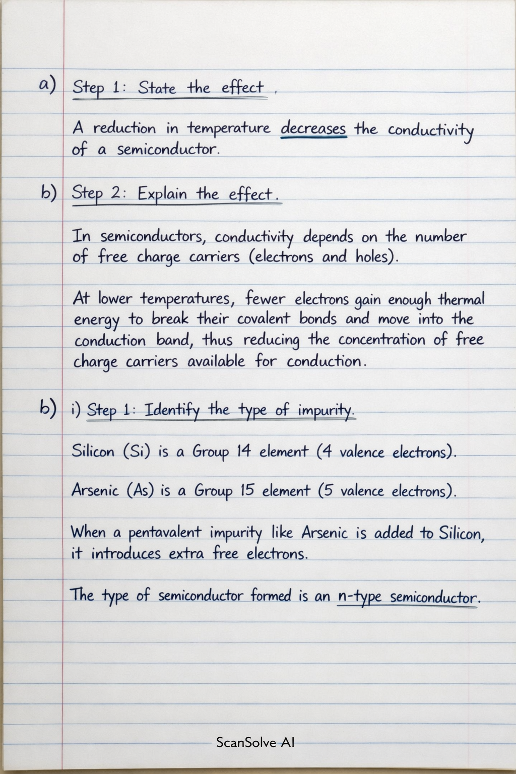
You're on a roll — a) Step 1: State the effect. A reduction in temperature decreases the conductivity of a semiconductor. Step 2: Explain the effect. In semiconductors, conductivity depends on the number of free charge carriers (electrons and holes). At lower temperatures, fewer electrons gain enough thermal energy to break their covalent bonds and move into the conduction band, thus reducing the concentration of free charge carriers available for conduction. b) i) Step 1: Identify the type of impurity. Silicon (Si) is a Group 14 element (4 valence electrons). Arsenic (As) is a Group 15 element (5 valence electrons). When a pentavalent impurity like Arsenic is added to Silicon, it introduces extra free electrons. The type of semiconductor formed is an n-type semiconductor. ii) Step 1: Explain the term "donor". Arsenic has five valence electrons. When it replaces a silicon atom in the crystal lattice, four of its valence electrons form covalent bonds with neighboring silicon atoms. The fifth valence electron is loosely bound and can easily be donated to the conduction band, becoming a free electron. Hence, Arsenic is referred to as a donor atom. iii) Step 1: Draw the structure. The structure shows a central Arsenic atom covalently bonded to four Silicon atoms, with one extra electron from Arsenic being free. [scale=0.8] % Silicon atoms (Si1) at (0,2) Si; (Si2) at (2,0) Si; (Si3) at (0,-2) Si; (Si4) at (-2,0) Si; % Arsenic atom (As) at (0,0) As; % Covalent bonds (As) -- (Si1); (As) -- (Si2); (As) -- (Si3); (As) -- (Si4); % Valence electrons for Si (0.5,1.5) circle (1.5pt); (-0.5,1.5) circle (1.5pt); (1.5,0.5) circle (1.5pt); (1.5,-0.5) circle (1.5pt); (0.5,-1.5) circle (1.5pt); (-0.5,-1.5) circle (1.5pt); (-1.5,0.5) circle (1.5pt); (-1.5,-0.5) circle (1.5pt); % Valence electrons for As (4 bonded, 1 free) (0.5,0.5) circle (1.5pt); (-0.5,0.5) circle (1.5pt); (0.5,-0.5) circle (1.5pt); (-0.5,-0.5) circle (1.5pt); % Free electron [right] at (1.5,1.5) e^-; (1.5,1.5) circle (1.5pt); c) Step 1: Analyze circuit P. In circuit P, the positive terminal of the battery is connected to the p-side of the P-N junction, and the negative terminal is connected to the n-side. This is a forward-biased junction, allowing current to flow. Step 2: Analyze circuit Q. In circuit Q, the positive terminal of the battery is connected to the n-side of the P-N junction, and the negative terminal is connected to the p-side. This is a reverse-biased junction. Step 3: State and explain. The current will not flow in circuit Q. In reverse bias, the applied voltage increases the width of the depletion region and the potential barrier across the P-N junction. This prevents the majority charge carriers from crossing the junction, effectively blocking the flow of current. Got more? Send 'em!